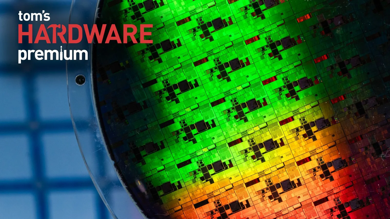
Export controls have kept ASML's most advanced EUV lithography machines out of China. Instead, the country's chipmaking industry has relied on less-capable deep ultraviolet (DUV) lithography machines. By using multiple exposures on critical chip layers, these older machines are still capable of producing performant silicon. However, as multiple patterns are applied there are more chances for defects, longer manufacturing times, and higher bills. Experts note that pushing DUV further introduces severe scaling challenges.
For years, extreme ultraviolet (EUV) lithography has been seen as China’s biggest choke point in the country’s attempts to build cutting-edge chips. The machines, made exclusively by Dutch manufacturer ASML, use 13.5nm-wavelength light to print some of the most intricate features found on modern processors. Sales of ASML’s EUV systems are subject to export restrictions, forcing Chinese manufacturers to squeeze ever more out of older deep ultraviolet, or DUV, lithography instead. The EUV gap alone between China and the West is at least half a decade, according to analysts.
But even without access to EUV machines, China has gotten surprisingly far in recreating what it offers through existing technology.
Teardowns of Huawei’s Mate 60 Pro in 2023 found the phone’s Kirin 9000S processor had been made by SMIC using a second-generation 7nm-class manufacturing process without EUV. More recently, analysis of Huawei’s Kirin 9030 found SMIC had pushed its DUV-based process closer still to the density associated with 5nm manufacturing – although it continued to lag behind the leading processes used by TSMC and Samsung.
Multiple Patterning
The trick is multiple patterning. Rather than trying to print an overly intricate chip layer in a single pass, Chinese manufacturers are dividing up the complex design into several simpler patterns. Repeat the process enough times and you can etch up something approximating the proper layer you intended.
The trick works. But according to lithography expert Chris Mack, co-founder and CTO of Fractilia, asking whether a chip can be made without EUV overlooks the trade-offs manufacturers make in order to do it.
When this transition first began, industry consensus suggested that cost-wise, three exposures on a 193 immersion tool cost about the same as one exposure on an EUV tool. At three exposures, costs were about even, but as soon as manufacturers hit four masks to replace a single EUV mask, EUV became more cost-effective.
It’s also likely to produce a higher quality product with fewer defects. Each time a wafer is patterned, that new pattern has to line up perfectly with everything that’s already been etched beneath it. The more individual exposures needed to produce a single layer, the more opportunities there are for things to go wrong as process variations accumulate.
Chip designers can try and avoid that by leaving more space around features so the finished processor can actually be manufactured reliably. But that means the chip ends up bigger – and bigger chips become expensive very quickly. Making each die larger means fewer fit on every wafer, and wafers cost tens of thousands of dollars each.
Manufacturers do not sell raw wafers; they sell functional dies. The economic equation depends entirely on how many dies fit onto a wafer and the final yield rate determining how many chips can actually be sold.
The Efficiency Gap
There is some evidence of what that efficiency gap can look like in practice, particularly in memory chips. In a June report, Morgan Stanley estimated that Chinese DRAM manufacturer CXMT was producing only around one-third as many bits per wafer as Western competitors. Analysts believe the older process node only accounted for part of that shortfall, pointing to lithography access as a hard ceiling on Chinese memory development.
It is also why claims that China has reached a particular semiconductor process node need to be treated with caution, as marketing terms often diverge significantly from physical realities.
That discrepancy is visible in SMIC’s latest chips. Reporting suggests its N+3 process represents meaningful progress towards 5nm-class manufacturing, but actual measurements show it remains significantly less scaled than established 5nm processes from Samsung and TSMC. That does not mean DUV has reached the end of its useful exploitation, however.
Stretching DUV's Efficacy
Micron serves as an example of how far DUV can be stretched, producing competitive DRAM chips using DUV, multiple patterning, and tight process control. Its 1-alpha generation of chips was developed without EUV, pushing 193nm immersion further than other memory makers to create competitive chips.
Morgan Stanley believes CXMT’s planned move to 1-alpha DRAM for HBM3e is achievable without access to EUV, citing Micron as evidence. Advanced packaging will also allow firms to use DUV to produce later generations of DRAM by the end of the decade.
Micron also designed its products around the manufacturing technology available to it, rather than simply trying to recreate an EUV process on older equipment. If the entire ecosystem of 193 immersion were fully available, manufacturers could optimize designs specifically for multi-patterning workflows.
Memory production relies on highly repetitive structures, making close coordination between chip design and manufacturing much easier than it is for complex logic processors found in phones and computers.
Memory production remains significantly less complex than advanced logic manufacturing.
Even Micron eventually concluded that EUV was worth adopting. Its newer 1-gamma DRAM process uses EUV lithography, helping the company achieve more than 30% greater bit density per wafer than its preceding 1-beta generation.
EUV is not a complete panacea either, as stochastic effects caused by low photon counts require higher exposure doses to improve pattern control, which quickly drives costs back up.
Consequently, experts believe there is an economic limit to how far multiple patterning can substitute for EUV. Achieving viable 3nm or 2nm nodes without EUV remains economically impractical.
That does not mean Chinese chipmakers will simply hit a technological wall and halt production. They can continue pushing DUV forward while accepting larger dies, lower yields, and longer manufacturing times.
Firms can also throw financial capacity at the problem. Morgan Stanley projects that CXMT will increase its global DRAM bit supply share through greenfield capacity investments despite remaining on a 1-alpha process without EUV. Similarly, heavy state support and new capacity are expected to raise China's AI chip self-sufficiency over the coming years, though advanced packaging, HBM, and software will leave a persistent technological gap compared to Western counterparts.