Breakthrough in Wafer-Scale Diamond
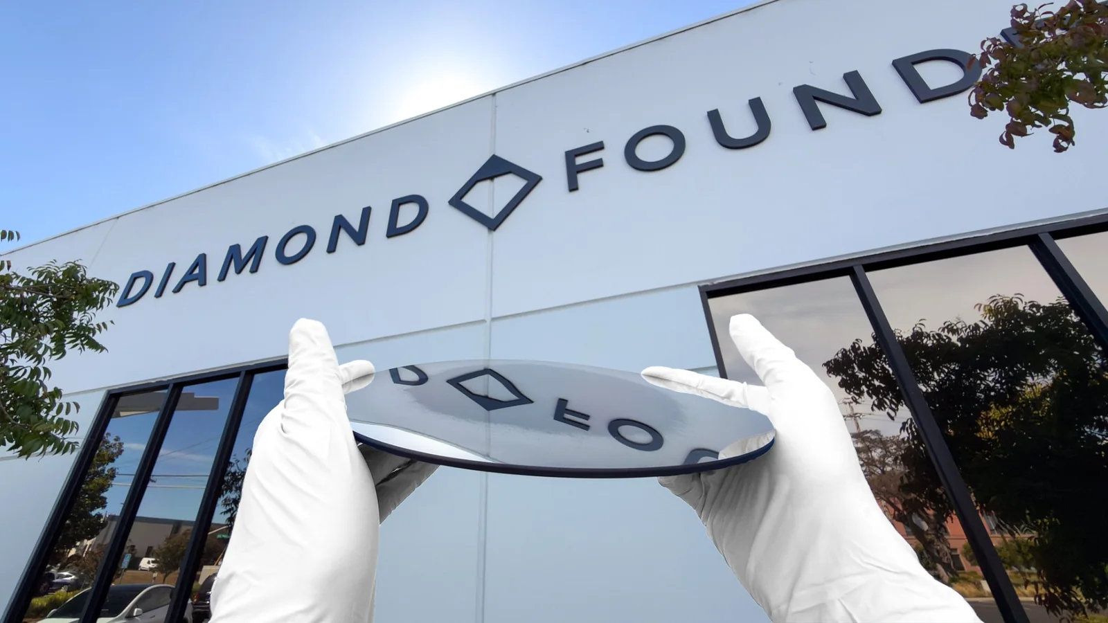
Diamonds have exceptional cooling capabilities due to their excellent thermal conductivity, with the material estimated to be at least five times more conductive than copper. Because of this, Diamond Foundry, a firm focusing on lab-grown diamonds, announced the world’s first 200mm single-crystal diamond (SCD) wafer. The 200mm SCD is about the same wafer size that semiconductor fabs use for older processes, with the company boasting on its website that single-crystal diamond has entered the wafer-scale era. This is part of the effort to manufacture SCD at scale so that it can be used for semiconductor cooling, especially now that increasing power of AI chips has also led to enormous thermal problems.
What makes Diamond Foundry’s 200mm SCD wafer different from other lab-grown diamonds is that it’s created as a high-quality single-crystal piece instead of a polycrystalline gem. Although the former is difficult to manufacture, it is what allows diamond to become an extreme efficient thermal conductor while simultaneously retaining its electrical insulating properties — this efficiency should help cut down on hotspots, making SCDs an excellent solution for AI chip cooling.
Production Roadmaps and Industry Context
The company also showed in a graph that it is now thought possible to create a D300 SCD wafer before 2030, matching the size of the wafers used in leading node processes. However, it should be noted that the sample shown by the company remains unpolished, meaning it still needs to go through some processes to make it suitable for chipmakers.
Although the company was founded in 2012, it also acknowledged the work of scientists who have been chipping away at the scale problem of SCDs since the early 2000s. This is one of those milestones that once seemed almost impossible. Hundreds of engineers, scientists, and technicians contributed to getting here. It is the accumulated result of countless experiments, failures, inventions, rebuilt machines, and insights over more than a decade, according to Diamond Foundry leadership.
Observers noted that researchers pursued this goal for 25 years against the prevailing view that single-crystal diamond simply could not be made at this scale. Today, that perseverance shows as the first-ever 200mm single-crystal diamond, making larger 300mm production more predictable as well.
Wider Industry Efforts in Diamond Cooling
Diamond Foundry isn’t the only company that has identified the potential of lab-grown diamonds for semiconductor cooling. Akash Systems secured $18.2 million in CHIPS Act funding in 2024 to produce Gallium Nitride fused with synthetic diamond, which it claims will reduce temperatures by 20 degrees C. The De Beers Group is also building a copper-plated diamond composite material aimed at improving cooling efficiency for AI, high-performance computing, and GaN RF devices. Even Frore Systems is diving into diamond-infused watercooling cold plates for Nvidia’s next-generation AI GPUs.