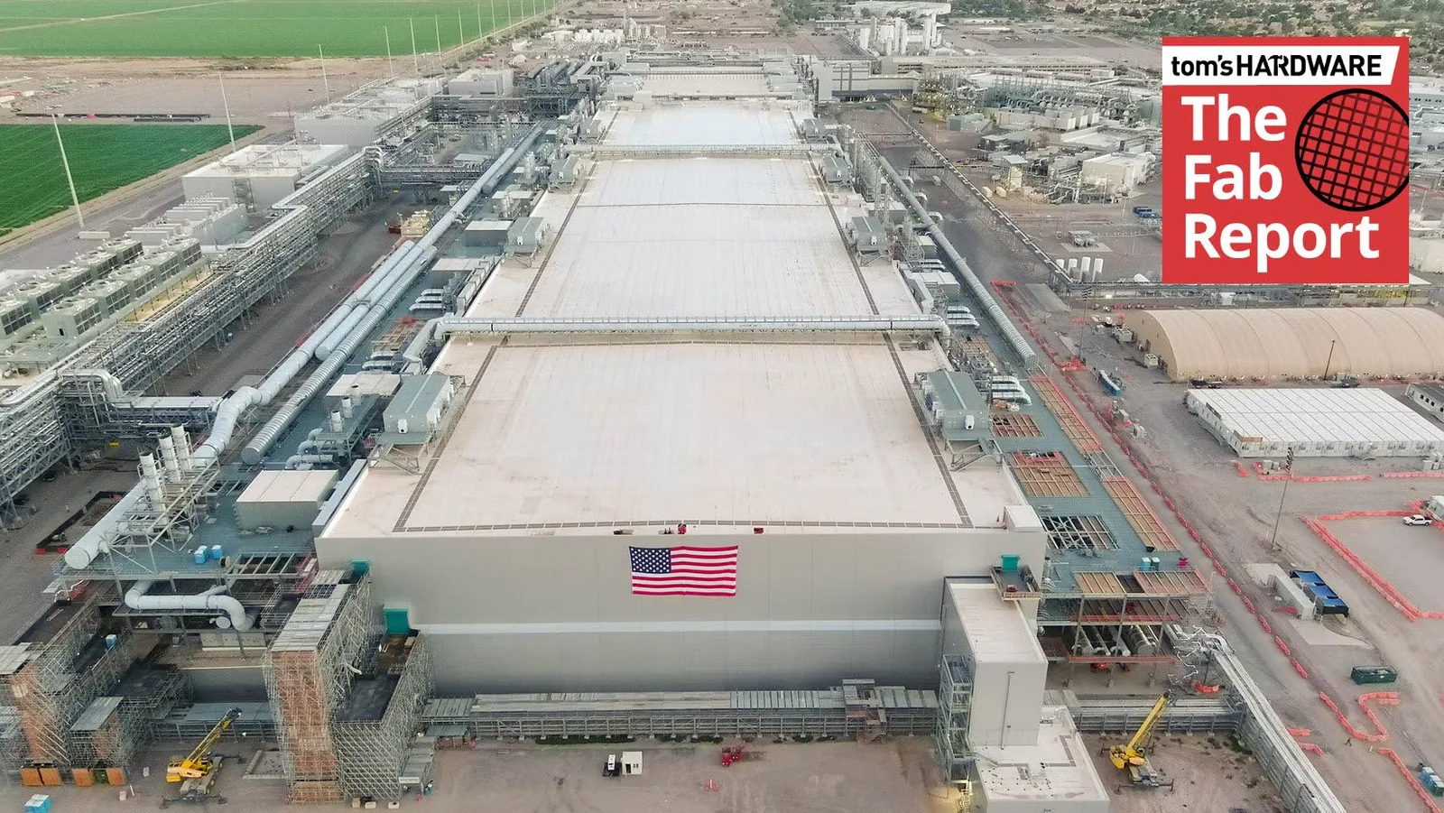
Fab 62 Tool Installation
Intel on Wednesday announced that it had started installing production tools at its Fab 62 in Arizona, and the fab is on track for mass production by late 2028. The company also reported progress on its Ohio One manufacturing complex and confirmed that it has integrated High-NA EUV lithography into high-volume manufacturing. Meanwhile, Intel continues to invest in its leading-edge process technology R&D, advanced packaging, and photomask production capabilities in the U.S.
Fab 62 to begin operations in 2028
Intel completed construction of its Fab 62 shell some time ago; now it is time for the company to begin installing production tools, which is what it is doing now. Intel expects the new facility to become operational before the end of 2028, although it has not disclosed when it intends to begin high-volume production or which nodes it will produce.
Intel has not officially assigned Intel 14A to Fab 62, although the facility has been discussed as a potential manufacturing site for the node. When Intel announced Fab 52 and Fab 62 in Arizona, it said the two facilities would manufacture its most advanced process technologies, including Intel 20A and 18A. Intel subsequently designated Fab 52 for Intel 18A manufacturing, while Fab 62 remains unassigned.
Given Intel's manufacturing process roadmap disclosed earlier this year, Fab 62 will be able to make chips on 18A, 18A-P, and 14A nodes. Intel currently manufactures Intel 18A chips at the neighboring Fab 52, whereas Fab 62 could potentially accommodate either additional Intel 18A capacity or the company’s next-generation Intel 14A process technology.
The facility will become Intel's Fab 62, the sixth high-volume semiconductor manufacturing fab at its Ocotillo campus, which has served as one of the company’s primary production sites for decades.
Intel has also not revealed Fab 62's planned wafer processing capacity, or the amount of capital expenditures required to complete the facility. Nevertheless, the installation of production equipment indicates that the project has progressed beyond construction of the building itself.
High-NA EUV Integration
Another noteworthy disclosure concerns Intel's deployment of High-NA EUV lithography. Intel was the first chipmaker to install a commercial High-NA EUV scanner at its D1X fab near Hillsboro, Oregon, and subsequently integrated the tool into high-volume manufacturing to produce its Panther Lake and other chips.
The Gordon Moore Park at Ronler Acres in Oregon is where Intel develops its most advanced logic process technologies and initiates volume production of the latest processors. Usage of High-NA EUV to produce select tiles for Panther Lake CPUs at D1X is a natural fit for the development fab, as it helps Intel to better understand how these lithography systems work.
Ohio One Complex
Intel has also made progress with its Ohio One manufacturing complex in New Albany, Ohio. Construction workers recently installed the first major structural truss at the site's first semiconductor fab, which represents a milestone in the development of the company's manufacturing operations in the state.
Unfortunately, Intel did not provide an updated construction schedule for Ohio One or disclose when the first fab is expected to begin operations. Intel also did not reveal which process technology the facility will eventually use or the estimated manufacturing capacity it will provide.
Advanced Packaging and Photomask
In addition to leading-edge manufacturing capacity in the U.S., Intel continues to invest in advanced packaging technologies. Oregon serves as the company's main research and development center for advanced logic and 3D interconnect technologies, while Arizona hosts advanced packaging R&D, assembly, and testing operations. Intel uses its site in New Mexico to produce its complex multi-chiplet processors relying on advanced packaging methods.
Intel recently broke ground on a new photomask manufacturing facility in Santa Clara, California. The new facility will be an important part of Intel's supply chain in the U.S., as the company will be the only chipmaker in America to develop and produce chips using leading-edge nodes completely domestically.
To highlight its supply chain, Intel disclosed that its U.S. operations involve more than 4,500 suppliers across 49 states, as its annual domestic expenditures exceed $29 billion. The company stressed that domestic semiconductor leadership requires not only wafer fabrication capacity but also research, process development, advanced packaging, and a comprehensive supply chain.