Development Milestone
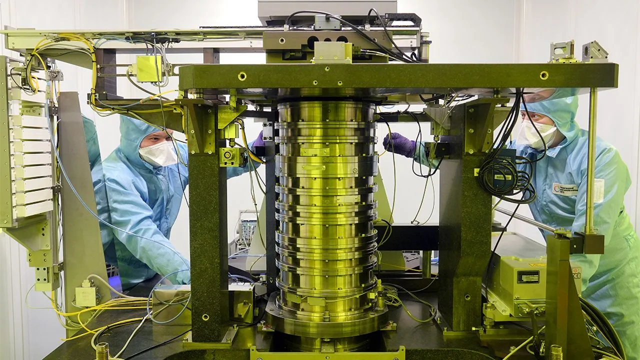
Russia-based Zelenograd Nanotechnology Center has completed the third R&D stage of the company's first lithography tool capable of processing 200-mm wafers using a 130nm process technology. The tool is currently being tested internally and is years away from being used at a real fab to produce chips in mass quantities. Observers suggest that while the device is promoted as a domestic 130nm-capable lithograph, component origins involve multiple collaborative efforts.
The creation of a prototype of a domestically developed photolithography system designed for a 130nm process is an important milestone for the region's microelectronics industry, according to industry analysts. It demonstrates the engineering expertise required to develop such equipment and paves the way for developing a range of systems targeting smaller process nodes such as 90nm and 65nm.
Partnerships and Funding
While Zelenograd-based ZNTC is responsible for the project, Belarus-based Planar handled the development of the lithography system. Planar manufactured mechanical assemblies and components and commissioned the prototype, while lasers for the unit were developed by Lassard. ZNTC oversees the overall system development, test and process equipment design, projection-lens calculations, and process modeling. The development program received approximately $70 million from state funding.
It is estimated that one 130nm-capable ZNTC stepper costs roughly $6.7 million, with its laser light source costing around $600,000, bringing the total tool cost to approximately $7.3 million. By comparison, historical equipment like ASML's PAS 5500/150 stepper launched with a list price of $3.1 million in 2001, which translates to roughly $5.8 million adjusted for modern inflation.
Node Context and Capabilities
While 130nm manufacturing processes were widely adopted by major western chipmakers in the early 2000s, local chipmakers have historically relied on lithography equipment from ASML for their 130nm-class nodes. Whether ZNTC's stepper can seamlessly integrate into existing nodes remains unverified, though the organization claims responsibility for process technology modeling and development, focusing on resists, exposure doses, masks, and alignment parameters rather than inventing an entire node from scratch.
Production Timeline
Given typical lithography tool development cycles, the 130nm stepper remains years away from actual chip production. The engineering prototype was delivered several months behind initial projections and must undergo extensive internal acceptance testing. Following this phase, developers must finalize designs and validate imaging, overlay, reliability, and throughput before commercial chipmakers can characterize and qualify the hardware for production flows.
Established lithography suppliers typically require several years to transition from initial integrated engineering systems to full production deployment. A realistic timeframe for the machine to process commercial wafers points toward 2029 at the earliest, though limited production of the steppers themselves could potentially begin sooner depending on parts availability.