Introduction to H-TPU
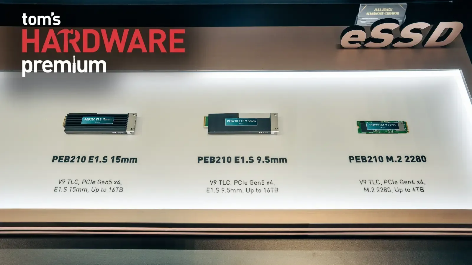
SK hynix has detailed plans to reduce reliance on power-hungry CPU cores with an in-house core named a Hynix Transaction Processing Unit (H-TPU). Not to be confused with an AI accelerator, an H-TPU would assist with repetitive work handled by an SSD, which usually demands more cores on a controller as drives get faster. These new cores are placed in clusters and would handle routine I/O with a four-stage, in-order pipeline, while management is left to the traditional Arm CPU. The new, tiny cores are claimed to draw only about 2.5% of a general-purpose CPU core’s power, with just around 4% of its area. Now, the company plans to apply H-TPU across its portfolio of products, according to industry reports.
Speaking at the International SoC Design Conference, company executives noted that SSD controller CPUs are reaching their limits on power and area. As PCIe bandwidth doubles every generation, controller CPU clocks and control capabilities struggle to keep pace. SK hynix plans to apply the H-TPU across its NAND products, including next-generation enterprise SSD controllers where high IOPS demands make the bottleneck most apparent.
The Scaling Challenge in SSD Controllers
This scaling issue is highlighted by the growing core counts in competing products. Marvell’s PCIe 6.0 Bravera SC6 uses 12 Cortex-R82 cores in two six-core clusters alongside three Cortex-M7 cores and a secure Cortex-M3. This represents a significant jump from its PCIe 5.0 predecessor, the Bravera SC5, which utilized 10 cores. Core counts have steadily climbed alongside faster PCIe speeds out of sheer necessity.
SK hynix’s alternative is its proprietary H-TPU, a small and programmable core accompanied by a dedicated compiler and development tools. It features a four-stage pipeline with sequential execution, avoiding out-of-order units. It is engineered specifically to process read and write commands, manage metadata, and handle buffer control.
Storage control involves over 100 distinct functions, rendering monolithic CPUs inefficient. SK hynix breaks these functions down across dozens of small TPU clusters, giving each H-TPU a specialized operational role. While the total number of H-TPUs exceeds 100, exact core distributions per cluster have not been disclosed.
Workload Distribution and Efficiency
The main CPU continues to handle error recovery, exception handling, and storage-policy management, meaning the H-TPU functions as a complementary offloader rather than a complete replacement. Unused cores drop into a low-power mode during idle periods.
Splitting storage workloads is an established industry practice. Phison’s CoXProcessor architecture pairs main CPU cores with hardened macros or micro-cores to offload repetitive firmware tasks at wire speed, an approach utilized in controllers like the E18 and enterprise-focused X1.
Patent Insights and Hardware Automation
Company patents reveal a structured split between control planes and I/O processing planes, organizing small processors into groups based on specific operational stages—such as host ingestion, caching, mapping, and NVM communication with the NAND—allowing the main CPU to step in strictly for exceptions.
In patent examples, these smaller cores utilize a fraction of the logic gates required by a standard CPU, maintaining flexibility through programmable firmware rather than rigid hardware circuits.
The subsequent phase of this architecture involves hardware automation (HWA), shifting command processing, address lookups, and buffer copies directly to dedicated circuits to maintain predictable completion times for high-IOPS enterprise drives.
SK hynix has previously explored fixed-hardware paths in various patent filings, describing dedicated write automation circuits capable of handling non-intelligent tasks while firmware retains complex duties like garbage collection.
Integration with Next-Gen Technologies
The H-TPU architecture is reportedly integrated into Nvidia's "Storage Next" project with SK hynix. Furthermore, the company plans to deploy it in high-bandwidth flash (HBF) products designed to stack NAND dies for AI inference, aiming to deliver high-bandwidth memory levels of performance paired with significantly larger capacities.
In HBF configurations, read operations vastly outnumber writes, requiring efficient buffer management and prefetching driven by AI compilers to mask underlying NAND latency.
While H-TPU has yet to debut in a commercial enterprise SSD controller, the transition toward specialized single-job processing units aligns with the mounting performance demands of modern AI-driven server environments.
As storage demands accelerate toward future PCIe standards, controller manufacturers must adapt beyond simple core scaling to maintain efficiency.