Tesla's Shift to Super Intelligence
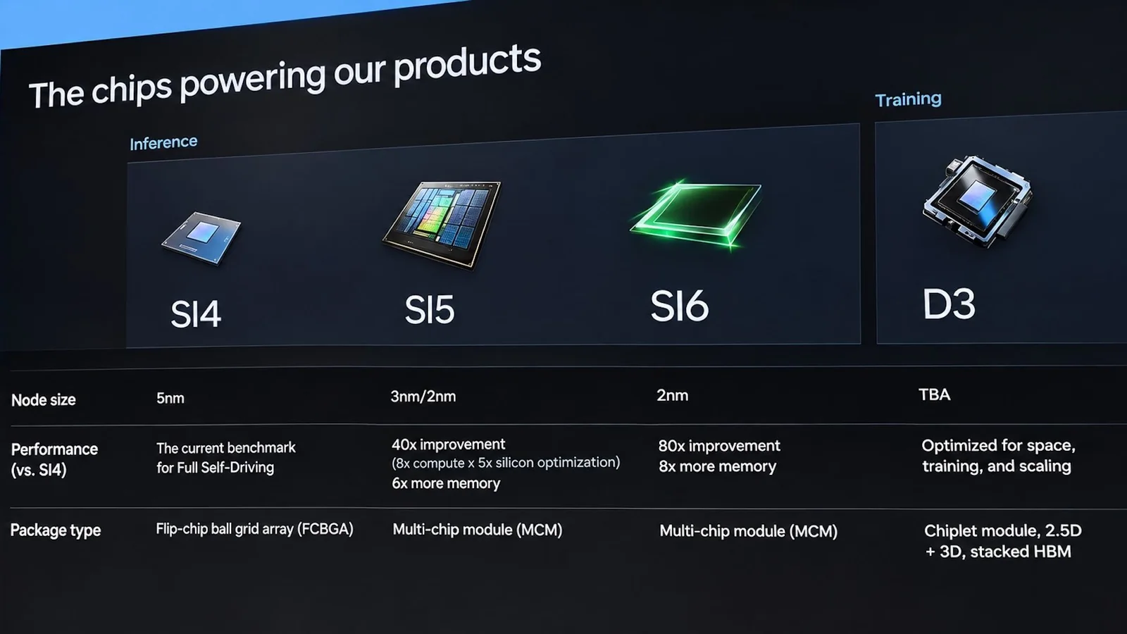
Tesla has disclosed its revamped AI accelerator roadmap that sheds some light on the future of the company's chip development efforts. The company expects that its 6th Generation inference accelerator will bring 80X more compute performance than the existing 4th Generation chip, whereas its D3 training accelerator will cease to use SRAM-centric architecture in favor of a multi-chiplet design with stacked HBM. Also, Tesla has adopted the term "super intelligence" instead of artificial intelligence for its AI accelerators, renaming them with SI monikers.
Wait a minute… I thought @elonmusk ’s Tesla chips were called AI4, AI5, and AI6. But in this latest presentation, they’re now labeled SI4, SI5, and SI6. Then I remembered: President Trump wants to replace “Artificial Intelligence” (AI) with “Super Intelligence” (SI). Looks like Elon Musk may already be embracing the new terminology. 🤔November 4, 2026
Dojo D3: No more wafer-level integration?
Perhaps the most interesting development in Tesla's AI hardware roadmap is the re-emergence of the in-house developed Dojo training accelerator. The 3rd Generation Dojo will be considerably different from the first two generations, Dojo D1 and Dojo D2.
Tesla describes its next-generation Dojo 3 (D3) training accelerator as a chiplet-based design that combines 2.5D and 3D packaging technologies with stacked HBM. This represents a substantial departure from the original Dojo D1 system-on-wafer architecture, which relied on distributed on-chip SRAM. The adoption of HBM suggests that Tesla intends to substantially increase memory capacity, as modern AI models consume extreme amounts of memory to store parameters, activations, and intermediate data.
Stacking HBM atop wafer-scale interconnected logic dies adds further design complexities, cooling challenges, manufacturing complexity, and long-term reliability concerns. While most of the challenges can be resolved by adding redundancy and refining process technologies, this all comes at a cost, making wafer-scaling less likely for D3.
Tesla has yet to disclose D3's compute performance, memory capacity, manufacturing process, or development schedule. It claims that its Dojo D3 will be optimized for 'space, training, and scaling,' which means the unit will offer decent performance and will be easy to scale. More intriguingly, the D3 is also set to be optimized for extraterrestrial deployments, which probably means radiation hardening for at least select SKUs.
SI6: 80X more performance than HW4 in a few years
Another interesting detail in the roadmap is the disclosure of approximate compute performance of Tesla's 6th Generation inference accelerator (SI6): 80X compute improvement over HW4 and 9X more memory over HW4. Depending on how HW4 performance is measured, this suggests 17,280 – 46,080 TOPS. Of course, these are estimates. To put the numbers into context, Nvidia's Rubin GPU offers 50 NVFP4 PFLOPS for inference, whereas SI6 is due in 2029 – 2030.
Tesla's existing 4th Generation inference processor used in the company's automobiles today is made by Samsung Foundry using its 7nm-class process technology and relies on conventional flip-chip ball grid array (FCBGA) packaging as well as presumably 16 GB of GDDR6 memory. The company describes the processor as the current benchmark for its Full Self-Driving (FSD) technology, which makes it the baseline against which performance of future generations is measured.
The upcoming 5th Generation inference accelerator called SI5 will be manufactured using 3nm- and 2nm-class process technologies at TSMC and Samsung Foundry, respectively, and will adopt a multi-chip module (MCM) design. Tesla expects SI5 to deliver a 40X performance improvement over HW4. The processor is expected to consume from 250W to 800W depending on application, and will feature six times more memory than its predecessor (i.e., 96 GB).
Moving on to the Tesla's 6th Generation inference accelerator (SI6), which is set to further increase compute performance to 80 times that of HW4 and feature eight times more memory than the current-generation processor. This could translate to 17.28 – 46.08 POPS and 144 GB of memory.
Tesla has already inked a deal with Samsung Foundry to make its 6th Generation inference accelerators through 2033, and the new slide reveals that the unit will be made using a 2nm-class process technology. Given the fact that the chip is due in 2029 – 2030, this likely refers to automotive-grade SF2A, performance-enhanced SF2P, or even SF2Z with backside power delivery.
SI6 will retain the multi-chip module (MCM) approach introduced with AI5/SI5/HW5, which seems rational as it will be able to leverage experience it is going to get with its 5th Generation inference accelerator and retain relatively reasonable packaging costs. It remains to be seen when Tesla adopts HBM for its inference accelerators, but probably not with SI6.