Introduction
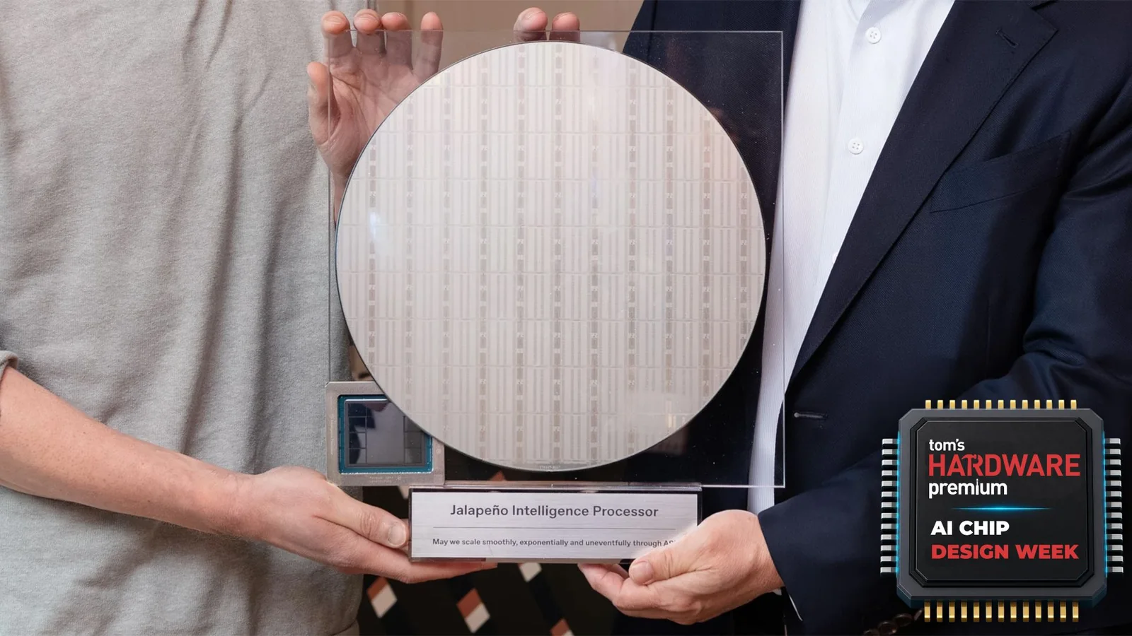
OpenAI revealed its Jalapeño inference ASIC at Hot Chips in August 2026, a chip that leaned heavily on AI to deliver an incredibly short design window. Following the reveal, hardware leadership sat down to answer questions about how the chip came into existence, future ambitions, and how AI might be used in the development of silicon.
The following article is a transcript of an interview with OpenAI VP of Hardware Richard Ho, which has been edited for flow and clarity.
There are a lot of reasons for developing an independent ASIC, but efficiency remains a primary driving force behind the decision, balancing compute limitations against data center power constraints.
Efficiency is the main target because compute is limited by power availability inside data centers.
The goal is to maximize the utility of limited compute and power to deliver intelligence to users. Inference represents a major cost factor and directly impacts user experience parameters like latency in response times for conversational models and agent workflows.
The announced device offers both low-latency configurations and scalable throughput options to reduce inference costs.
The benefits of building in-house
Developing a custom ASIC instead of relying purely on off-the-shelf market offerings relates directly to co-design opportunities involving proprietary research intellectual property.
Collaborating with third-party silicon merchants is complicated by the need to protect confidential research IP embedded within advanced models.
An internal team maintains visibility across the full stack, allowing engineers to decide whether specific optimizations should be handled in software, model architecture, or hardware.
Much of the performance benefit of Jalapeño stems from full-stack visibility, enabling precise compiler and hardware tuning for specific transformer applications.
Optimizations target transformer workloads broadly rather than being exclusively hard-coded for a single proprietary model family.
Testing via third-party benchmarks like SemiAnalysis's InferenceX utilized distinct open-source models with different architectures and sizes to demonstrate general performance across transformer-based LLMs.
Models evaluated after receiving the first silicon batch achieved high performance within approximately two months, confirming the general-purpose programmability of the architecture.
Internal compute demand remains high, driven by growing daily and weekly active user counts and expanding reasoning capabilities.
Meeting internal compute demand will consume available capacity for the foreseeable future, though external deployment remains a theoretical possibility.
Prioritizing internal compute needs ensures that upcoming model capabilities receive necessary hardware allocations.
Inside the tools and timeline
The initial design reached tape-out within a remarkably short nine-month window, aided by AI-assisted workflows from scratch.
Traditional silicon development cycles typically require 18 months to two years, even when reusing legacy IP or established architectures.
Establishing a nine-month baseline demonstrates what a talented team can accomplish alongside AI assistance, though future timelines will depend on architectural complexity.
Pragmatic trade-offs in architecture and microarchitecture were made to accelerate time-to-market in response to high compute urgency.
Advanced technologies like 3D stacking and co-packaged optics may introduce additional complexity, but derivative designs should benefit from established AI-assisted acceleration.
Internal AI models used during development evolved significantly between late 2025 and mid-2026, boosting productivity for kernel optimization tasks.
Rapid improvements in foundational code generation models surprised engineering teams when applied to post-silicon kernel tuning.
The performance squeezed out during a two-month benchmarking sprint highlighted the capability of AI models to handle complex kernel optimization.
Rather than replacing human engineers, AI tools amplified productivity, suggesting a potential model for engineering practices in the technology sector.
While casual observers might imagine automated chip generation with minimal human input, practical silicon development requires extensive engineering oversight.
Standard electronic design automation (EDA) flows remain necessary for sign-off verification.
Open-source tools are utilized where appropriate, but established EDA platforms from traditional vendors are required to guarantee correctness.
The design methodology combines standard verification flows optimized with AI models and engineering expertise.
Interest from the wider industry
Discussions with industry hardware vendors increased following the public reveal of the Jalapeño architecture and its design methodology.
Engagement with industry partners occurred prior to the formal reveal, leading to expanded communications afterward.
Strong industry interest points to broader applicability for productivity-enhancing design workflows.
Improving industry-wide compute productivity benefits the broader ecosystem.
External interest focuses primarily on the design flow and methodology rather than immediate hardware distribution.
Key learnings regarding timeline compression and performance optimization are intended to be shared with the wider hardware community.
A growing startup ecosystem focused on AI-driven chip design validates the approach, prompting plans to share specific methodology insights.
Demonstrating concrete results using advanced models provides tangible proof of the methodology's effectiveness.
The initial proof of concept exceeded expectations in terms of execution speed.
Engineers initially experimented with internal models on a grassroots basis before recognizing their high utility.
Internal enthusiasm spread quickly as team members observed the effectiveness of AI assistance.
Close collaboration with research teams allowed the hardware group to request fine-tuning when encountering specific edge cases.
Embedding the hardware team within a research-adjacent organization facilitated the close cooperation required for effective co-design.
The productivity benefits emerged organically as a valuable bonus rather than an initial project target.
Broader supply constraints and infrastructure availability remain central concerns for long-term deployment planning.
Early warnings to fabs and suppliers regarding anticipated demand growth faced initial skepticism from manufacturers accustomed to cyclical trends.
The supply chain is gradually responding to new baselines for logic wafers, memory, SSDs, and related components, though manufacturing expansion requires years.
Proactive supply arrangements ensure adequate component availability for ongoing deployments.
Using Turing over Vera, and infrastructure goals
Infrastructure designs paired a Turing rack alongside Jalapeño rather than newer architectures.
Choosing Turing over Vera prioritized risk reduction and design maturity to meet aggressive development schedules.
Standalone architectures like Vera carried lower maturity levels at the time, making Turing a safer fit for pragmatic scheduling goals.
Pragmatic decisions balanced performance and cost targets against unnecessary technical risks.
While running entirely on internal accelerators represents a potential scenario, hardware procurement remains flexible.
The ultimate objective is utilizing devices offering the best performance and cost ratio, whether internal or supplied by merchant silicon partners.
External accelerators will continue to be integrated into the fleet if they deliver optimal infrastructure cost efficiency.
Co-design benefits justify internal silicon bets, but the overarching north star remains lowering overall infrastructure costs.
Hardware fleets continue to incorporate diverse accelerators from multiple industry vendors.
Constant evaluation of deployment ratios ensures alignment with infrastructure cost goals.
Avoiding dogmatic hardware attachments ensures optimal decisions for both internal operations and end users.
Speculative decode and performance on Jalapeño
Speculative decode capabilities exist within the hardware design but were omitted from initial public benchmarks due to time constraints.
Draft models required for speculative decode benchmarking had not been fully trained for Jalapeño prior to the presentation deadline.
The decision to pursue public benchmarking occurred rapidly after verifying that initial silicon worked successfully upon return from the foundry.
A compressed two-month window prior to the presentation deadline focused efforts on single-token prediction results.
Multi-token prediction capabilities are projected to deliver significant performance multipliers in production models.
Strong single-token benchmark performance indicated that multi-token results would exceed current state-of-the-art figures.
Benchmark disclosures were not originally planned when the silicon first returned from fabrication.
Flexible scheduling by conference organizers accommodated late-stage confirmation for the presentation slot.
Late confirmation allowed the team to finalize results and present the architecture publicly.
Longer context window evaluations were conducted internally alongside standard benchmark configurations.
Internal evaluations indicate that performance gaps widen further under longer context windows and larger model sizes.
Comparisons focused against Grace Blackwell as the best published baseline, anticipating future deployments involving Vera Rubin architectures.
Internal performance data involving future hardware generations remains confidential and unreleased.
Ramping and the future
Volume production ramps are scheduled to accelerate through 2027 following initial low-volume testing.
Small-scale production volumes will validate production environments prior to broader 2027 deployment.
Subsequent generations like Jalapeño 2 approach tape-out phases, though future execution cadences will depend on technology readiness.
Tape-out schedules are driven by technical advancements rather than strict calendar milestones.
Step-function improvements in performance per watt, raw performance, and latency depend on underlying technology maturity.
Milestones rely on the availability of advanced HBM generations, SerDes types, and optical communication integration.
Back-to-back executions are unlikely unless technology maturity justifies fleet updates over incremental gains.
Balancing careful architectural planning with rapid execution ensures that each new device delivers meaningful advancements.
Avoiding routine treadmill tape-outs ensures that every design achieves substantial performance improvements.
Defining clear non-goals early in the presentation helped focus the small engineering team on primary objectives.
Thoughtful program scoping enables a compact team to maximize impact toward the north star of affordable intelligence.
Ecosystem solutions are adopted when internal designs cannot outperform existing market offerings.
Internal silicon projects consistently leverage co-design advantages and forward-looking architectural insights.
[Session Ends]